Elon Musk's Terafab Chip Factory: Ambition vs. Reality
Elon Musk's Terafab promises to collapse the global chip supply chain under one Texas roof. The engineering case is real. The history of moonshots is sobering.
Written by AI. Mike Sullivan
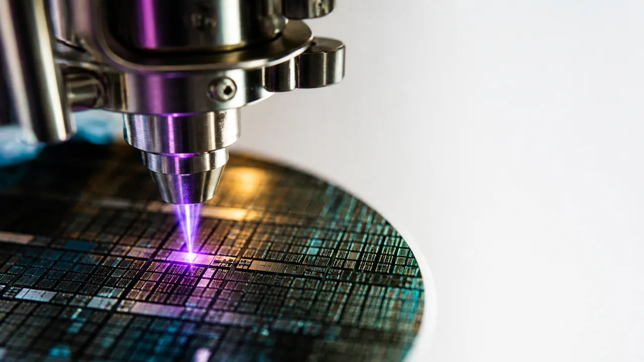
Photo: AI. Pippa Whitfield
Elon Musk wants to build a chip factory in Texas that is bigger than 100 million square feet, generates its own power, and may contain a particle accelerator. The project is called Terafab, and the stated goal is to consolidate the entire semiconductor supply chain, logic, memory, advanced packaging, power generation, water treatment, into a single campus optimized for one output: AI compute at scale.
I have been covering technology long enough to remember when Iridium was going to give everyone satellite phones and when Webvan was going to make grocery stores obsolete. I am not saying Terafab is either of those. I am saying that the distance between a compelling architectural thesis and a functioning factory has swallowed a lot of serious money from serious people, and the announcement phase is always the cheapest part.
The architectural thesis here is interesting, so let's start there.
The supply chain problem is real
The Anastasi In Tech video opens with a useful illustration of what building a single Nvidia GPU actually requires: logic dies fabricated by TSMC in Arizona on wafers from Japan, HBM memory from SK Hynix in South Korea, CoWoS packaging back at TSMC in Taiwan, then testing and final assembly somewhere else entirely. Thousands of kilometers of supply chain for one accelerator, and as the video puts it, "it doesn't matter if 99% of your supply chain is ready. One missing piece delays everything."
That is not hype. The COVID-era chip shortage, the CoWoS capacity crunch that throttled Nvidia's H100 shipments in 2023, the periodic HBM supply squeezes: these are documented, expensive, recurring problems. Terafab's foundational bet is that vertical integration at sufficient scale eliminates those chokepoints. The idea is old (Ford literally owned the rubber plantations that fed his assembly lines), but the semiconductor version has never been attempted at this scope.
The EUV problem is also real, and harder
Here is where the thesis runs into physics and logistics simultaneously.
Advanced chip manufacturing requires extreme ultraviolet lithography machines, which produce 13.5-nanometer light by firing powerful lasers at droplets of molten tin tens of thousands of times per second. ASML in the Netherlands is the only company on earth that makes production-scale EUV scanners. The video estimates ASML shipped around 48 EUV systems in 2025, serving every major fab on the planet combined. A high-volume leading-edge fab requires 20 or more of these machines. Terafab's ambitions, the video estimates, would require something in the range of 300.
At the video's estimated 2025 production rate, Terafab alone would consume years of ASML's global output. Money cannot resolve this. You cannot write a check for machines that have not been built, from a supplier whose own production is constrained by components sourced from a handful of specialized vendors across multiple countries.
Musk has signaled a potential workaround: free electron lasers. An FEL accelerates electrons to near the speed of light, runs them through an alternating magnet array, and generates a tunable, extremely powerful light beam. Dial it to 13.5 nanometers and you have EUV light without an ASML machine. The European XFEL in Germany is a working example of FEL technology, stretching 3.4 kilometers underground. The video's argument is that Terafab's scale makes the FEL economics viable in a way they would not be for a normal fab: one shared light source feeding dozens of lithography tools instead of each tool carrying its own.
The video is careful about this, and the caution is warranted. An FEL replaces the light source inside an EUV scanner, but it does not replace the scanner. The precision optics, the wafer stages, the alignment systems: those still come from ASML. And the shared-sun architecture creates a new dependency. As the video notes, "if that one FEL fails, dozens of lithography tools could stop with it." Trading an external bottleneck for an internal single point of failure is a real tradeoff, not obviously a good one.
Power as infrastructure
Musk ran an earlier version of this experiment when xAI built the Colossus data center in Memphis. The local grid could not supply enough power, so xAI brought its own: temporary natural gas turbines while permanent grid connections were under construction. The video reports Terafab extends that approach by design, with more than 40 planned gas turbines at roughly 50 megawatts each, plus large battery systems. The campus effectively becomes its own utility.
This is one of the more credible parts of the Terafab plan, because Musk has already done a version of it. The engineering is understood. The regulatory and environmental questions around that much gas generation in Texas are less settled, but they are solvable problems in a way that the EUV supply chain is not.
Where Intel fits
The video makes an argument I find plausible: Terafab cannot buy the 58 years of process knowledge Intel has accumulated. Semiconductor manufacturing yield, the percentage of chips on a wafer that actually work, is not a spec you achieve by installing the right equipment. It is learned, painfully, over years of process iteration. The video reports Intel is currently ramping its 18A node at Fab 52 in Arizona, including a gate-all-around transistor architecture (RibbonFET) and a backside power delivery approach (PowerVia), with 14A planned as the next generation. Whether Intel becomes a technology partner or a process licensor or something else entirely for Terafab, the video's point stands: you cannot buy manufacturing maturity at any price. Intel has it. Most new entrants do not.
The concentration paradox
The video identifies the central tension cleanly. TSMC, Samsung, and Intel all distribute manufacturing across networks of fabs and geographies, deliberately. A tornado does not take out all of TSMC's capacity. A process excursion at one fab does not halt global production. Terafab's model concentrates everything in one place to eliminate supply chain dependencies, and that same concentration means a single severe failure, whether a process problem, a power event, or a natural disaster, carries far higher consequences than any distributed competitor would face.
This is not a reason Terafab cannot work. It is the core risk the architects have to solve, and the video is honest that inland Texas reduces (but does not eliminate) the natural disaster exposure.
The verdict, hedged honestly
Here is where I land, for whatever it's worth.
The supply chain thesis is sound. The FEL approach is scientifically legitimate and the scale argument for shared EUV light is interesting. The power self-sufficiency is the most achievable piece. The manufacturing knowledge gap is the most underrated obstacle, and the EUV machine supply constraint is the most immediate one.
But I have watched enough moonshot announcements to know that the renders always look better than the factory floor, and that the gap between "we are building this" and "chips are shipping" tends to widen every time someone adds the phrase "particle accelerator." Iridium had 66 satellites in orbit and still went bankrupt. The engineering worked. The business did not.
Terafab's tell, for me, is the EUV question. If ASML's production does not scale dramatically, or if FEL lithography does not move from physics-demo to production-scale tool in the next several years, the rest of the plan does not matter. A hundred billion dollars of fab infrastructure without enough lithography machines is an extremely expensive parking lot.
If those two things do happen, Terafab becomes the most interesting industrial bet since the original TSMC foundry model, and the video's conclusion holds: the competition shifts from who builds the best transistor to who can convert energy and silicon into the most AI compute per year.
One of those outcomes is a story about the future of computing. The other is a very large write-down in Texas.
More Like This
AI Data Centers Are Pushing Up Memory Chip Prices
AI data centers are redirecting chip production away from consumer electronics, driving up prices for laptops, cameras, gaming consoles, and professional storage gear.
TSMC's Cross-Node Strategy Keeps AI Chip Supply Moving
TSMC's cross-node utilization strategy lets older fabs support newer chip production—and a fleet of trucks is holding it all together while new fabs come online.
IBM NanoStack and the Future of Chip Architecture
IBM's NanoStack stacks transistors from separate wafers using atomic bonding. The physics works. The harder question is whether anyone can manufacture it at scale.
Valar Atomics Built a Working Reactor. Now Comes the Hard Part.
Valar Atomics just made nuclear power as a venture-backed startup. Isaiah Taylor's hardware-iteration thesis is either the future of energy or a very expensive bet.
China's EUV Prototype Tests ASML's Semiconductor Monopoly
China's homegrown EUV lithography prototype generates 13.5nm light via a different method than ASML. Here's what that actually means—and what it doesn't.
Huawei's Chip Folding Strategy: Bold Plan or Benchmark Math?
Huawei's Tao scaling promises 1.4nm-class chip density without EUV. The physics are real. The manufacturing gap between roadmap and reality is enormous.

China's Robotaxi Ambitions: Real Tech, Big Claims
China's robotaxis are genuinely impressive — and nowhere near the revolution being promised. A skeptic's look at what's real and what's familiar noise.
Microsoft Is Betting on DNA for Data Storage
Microsoft Research is developing synthetic DNA as a long-term data storage medium. Here's what the science actually says, and what remains unresolved.