IBM NanoStack and the Future of Chip Architecture
IBM's NanoStack stacks transistors from separate wafers using atomic bonding. The physics works. The harder question is whether anyone can manufacture it at scale.

Written by AI. Mike Sullivan
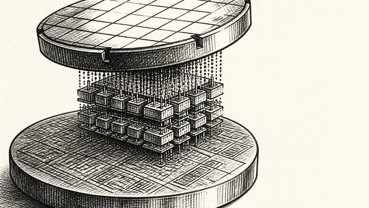
Photo: AI. Eira Pendragon
IBM has a long and storied history of announcing things that make the physics community sit up straight and the product roadmap community quietly change the subject. OS/2. Deep Blue. Watson. The 7nm research chip in 2015, which was genuinely impressive and genuinely not what you're running your workloads on today. So when the company announced what it's calling the world's first 0.7 nanometer chip — the NanoStack architecture — I read the press materials with the same combination of genuine interest and ambient wariness I've developed over several decades of watching IBM's research division operate in a different timezone from IBM's sales division.
Here's the thing, though: the underlying idea is not hype. It's something weirder and more interesting than hype.
The problem nobody wanted to say out loud
For sixty years, the semiconductor industry ran on one playbook: make the transistor smaller. It worked. We went from transistors you could see with a decent magnifying glass to structures measured in nanometers — and those nanometer numbers, as chip design engineer Anastasi covers in a recent video on the announcement, have themselves become a kind of fiction. "Those numbers haven't described the physical size of a transistor for years," she explains. "They are in fact technology generation labels, representing the overall capability of the process, like the performance and the drive current, rather than one particular dimension."
Which is a polite way of saying that the nanometer race has been partly a branding exercise for the better part of a decade. TSMC's "3nm" node and Intel's "3nm equivalent" don't literally have 3-nanometer features in the way that Intel's 90nm node in the early 2000s had 90-nanometer features. The labels survived because the industry needed a legible way to talk about progress, and "we've improved transistor density and power efficiency through a combination of architectural and materials innovations" doesn't fit on a product slide.
NanoStack doesn't try to win the nanometer race. It changes what the race is for.
What IBM actually built
The NanoStack announcement centers on a chip image taken with an electron microscope that, at first glance, looks like a single transistor. Look closer and it's two — one stacked directly on top of the other, fused together from what started as two completely separate silicon wafers. The channels where current flows are, as Anastasi describes them, "only about 15 silicon atoms wide." That's not the breakthrough, though. The breakthrough is that thin white line between the two transistors — the bonding interface — and the manufacturing logic that produced it.
The traditional approach to stacking transistors runs into a specific and nasty problem: building the second transistor on top of the first means running the entire wafer through hundreds more manufacturing steps, including repeated heating cycles that can reach over 1,000 degrees Celsius. At those temperatures, atoms in the already-finished transistor below start moving. Materials react. Tiny changes accumulate. The first transistor degrades quietly while you're trying to build the second one. As Anastasi puts it: "imagine finishing a skyscraper and then discovering that adding just one more floor could collapse the entire building."
IBM's answer was to stop trying to build both transistors on the same wafer. Instead, they manufactured each one independently — one transistor per wafer — and only attempted to fuse them after both were complete. The fusion mechanism is van der Waals forces: when two atomically smooth surfaces get close enough, the attractive forces between individual atoms, negligible in isolation, become collectively strong enough across trillions of contact points to hold an entire wafer together. Apply heat, and transient van der Waals attraction converts into stable chemical bonds. Two wafers become one device.
"It sounds elegant," Anastasi says, "but actually making it work took decades."
The part that isn't physics
That sentence does a lot of work. The physics of van der Waals bonding has been understood for a long time. What wasn't understood — or rather, what wasn't solved — was the manufacturing infrastructure required to make it reliable at production scale.
Consider the dust problem. A particle smaller than a red blood cell landing between two wafers before bonding will create a void, destroying the interface across a radius far larger than the particle itself. The entire elaborate choreography of cleanroom engineering — the polishing, the vacuum chambers, the chemical cleaning protocols — exists to prevent that one event. And then, after all of that, engineers have to align billions of transistors across two separate wafers without being able to directly see a single one. "There isn't a second attempt," Anastasi notes. "If they're wrong, the wafers are gone."
This is worth sitting with, because it's where the story stops being about IBM specifically and starts being about the manufacturing ecosystem that would have to scale this. Anastasi names two companies to watch: EV Group, the Austria-based wafer bonding equipment specialist whose portfolio specifically includes the precision bonding tools this kind of manufacturing requires (evgroup.com), and Tokyo Electron. Her read is that "the companies I will be watching more closely aren't IBM, but Austrian EVG Group and Tokyo Electron. Because when this technology becomes the future, their machines will be the ones making it possible."
That's the right frame. IBM Research has always been exceptionally good at solving problems that the rest of the industry then has to figure out how to actually build — which is a compliment, not a dig, though it rhymes with a dig if you squint. The question NanoStack raises isn't whether the physics works. IBM has apparently demonstrated that it does. The question is whether the manufacturing yield, at volume, at cost, makes this viable outside a research fab.
Why the density argument matters more than the specs
Stacking transistors the NanoStack way doesn't just mean more transistors per chip — it changes the geometry of what a chip can do. Anastasi's key insight here is about memory and logic proximity. AI processors, she argues, spend most of their energy not computing but moving data between memory and logic. "If we can bring that memory physically closer, suddenly the process spends less time waiting and less energy moving information around."
This is where the shift from "smaller transistors" to "denser compute" becomes a meaningful change in direction rather than a semantic one. If your constraint is the energy cost of data movement rather than raw transistor count, then stacking memory and logic in the same physical die — which NanoStack's wafer bonding approach enables — solves something that simply shrinking the transistor cannot. You're not just doing more with the same space; you're doing a different kind of thing with it.
Wafer bonding, as Anastasi notes, already appears in camera sensors, high-bandwidth memory for GPUs, and NAND flash storage. The technique isn't new. What IBM did was push it down to a level where the bond interface lives inside the transistor stack rather than between finished chips. That's not an incremental extension of an existing idea. It's the same idea operating at a different level of the stack — which, to anyone who's ever watched an architectural pattern propagate through an industry, has a familiar smell.
I remember watching Watson beat Ken Jennings in 2011 and spending approximately six months wondering if this was genuinely the inflection point everyone was about to say it was. It wasn't, in the way people meant it at the time. But it also wasn't nothing — the underlying work on natural language processing fed directly into things that did matter, on timelines nobody predicted. NanoStack might have a similar trajectory: not the thing itself, but the proof-of-concept that forces the manufacturing infrastructure to catch up.
What the scaling question actually means
"In the semiconductor industry, coming up with the idea has often been the easy part," Anastasi says. "Mass producing it changes the world."
That's where this lands, for now. NanoStack is a demonstrated architecture with a plausible density advantage and a manufacturing challenge that is genuinely hard, not just complicated. The companies that make the bonding equipment will have as much to say about NanoStack's future as IBM does. The cleanroom protocols, the alignment tolerances, the yield rates at volume — those are the variables that convert a research result into a product roadmap.
IBM has shown the architecture can work. The next question belongs to the fabs and the equipment suppliers, and it's a much slower, less photogenic process than the electron microscope image that kicked this whole conversation off.
The thin white line in that electron microscope image is either a preview of that era, or a very expensive research artifact.
More Like This

Do You Really Need an $80 HDMI Cable? Maybe Not
Tech reviewer Adam tests a premium HDMI 2.1 cable. We examine what you're actually paying for and whether most users need it.

Can Unreal Engine 5 Run on a $500 MacBook? Sort Of.
Testing Unreal Engine 5.7 on the MacBook Neo reveals what happens when professional software meets budget hardware—and why friction matters.
Intel's 18A Chip: A $20B Bet That Breaks Every Rule
Intel's Fab 52 is producing chips with two radical innovations at once—something the industry never does. Here's why that's either genius or catastrophic.

Microsoft Majorana 2: Bold Claims, Thin Evidence
Microsoft's Majorana 2 chip promises a 1,000x reliability leap and a 2029 quantum computer. Scientists say the paper doesn't back any of it up.

Nvidia's Autonomous AI Agents: What Actually Shipped
Nvidia announced NemoClaw, Nemotron-3 Ultra, and OpenShell at GTC Taipei. Here's what the technology actually does—and what questions it leaves open.

Huawei's Chip Folding Strategy: Bold Plan or Benchmark Math?
Huawei's Tao scaling promises 1.4nm-class chip density without EUV. The physics are real. The manufacturing gap between roadmap and reality is enormous.
Inside the Smartphone: 120 Years of Hidden Engineering
Professor Hannah Fry tears apart a modern smartphone to trace 120 years of engineering history — from Marconi's radio waves to a 200-million-pixel camera sensor.

Pokémon Go at Ten: AR's One Durable Success Story
Pokémon Go turns ten this week. A look at what it actually got right—and why the AR industry it was supposed to launch mostly didn't follow.