AI in Chip Design: Hype, Reality, and What Comes Next
Kimi's K3 model designed a chip autonomously. OpenAI's Jalapeno got built by a team of 20. What's AI actually doing to chip design, and what can't it touch yet?

Written by AI. Yuki Okonkwo

Photo: AI. Henrik Solberg
Kimi's K3 model dropped in July 2026 and, among other things, included a claim that the AI designed a chip in a single autonomous 48-hour run. EDA company stocks fell on the news. Hot Chips, OpenAI's first custom silicon called Jalapeno, agentic workflows everywhere you looked. The semiconductor world is having its AI moment, and it is moving fast enough that Asianometry's Jon Y, who attended both Hot Chips and Semicon Taiwan to report on all of this, admitted on camera that he was worried something would come out the week after posting that would make everything he said obsolete. Relatable content, honestly.
Before getting into what AI is actually doing in chip design, it helps to know what chip design even is. EDA (electronic design automation) is the software layer that makes chips possible. At the front end, engineers write RTL (register transfer level) code, basically a description of how data flows through logic. That gets synthesized into a netlist of gates. At the back end, physical design tools place those gates on a circuit and route the wires between them. Verification tools run throughout to check that the design does what it's supposed to do. Synopsys, Cadence, and Siemens are the dominant commercial players here. OpenRoad, launched in 2018, is the most prominent open-source alternative, integrating dozens of smaller tools to get you from RTL to a manufacturable GDSII layout file.
The gap between open-source and proprietary EDA is not a small one. According to Semiconductor Insight, open-source tools are proving capable for mid-range nodes and research chips, but are not yet competitive with commercial tools at the bleeding edge. A big part of why AI has struggled to crack chip design is this exact gap: process design kits (PDKs), the secretive IP bundles that encode how a foundry's manufacturing process actually behaves, are locked under NDAs so tight that neither the foundry nor the EDA maker can open-source them. Training data for AI has to come from what's publicly available, which means it's drawn from the weaker open-source side of that gap. The AI is, in effect, learning chip design from a textbook while the real work happens in a locked room.
What Kimi actually did (and didn't do)
Kimi's K3 technical report describes a small inference accelerator chip called the Nano KPU, designed using open-source EDA tools and the Nangate 45nm open cell library. The key claim from their report: "Within the 4 square millimeter analytical area budget, the design closes timing at 100 megahertz and achieves an RTL simulated decode throughput of over 8,700 tokens per second, integrating 1.46 million standard cells, 0.277 megabyte of SRAM, and an int4 macro array with fused dequantization."
Jon Y's breakdown of the caveats here is sharp. The K3 design got functional verification, but skipped cell placement, routing, physical verification, and sign-off. The timing closure claim is an estimate. And 100 MHz on a 45nm open-source library is not impressive performance; human-designed chips on the same library can range from 20 MHz up to around 450 MHz, and commercial 45nm processes can push 1 to 3 GHz depending on power and design constraints.
Kimi knows this. Their stated point is that the agent achieved functional completeness autonomously. Jon Y's read on it: "people should not miss the forest for the trees. This is directional. It smells like the future."
Fair. But the forest and the trees both matter when you're deciding whether to restructure a whole industry around this technology.
Christina Lee's loops and why they matter
The most interesting thing in Jon Y's video is his description of a post by Christina Lee, former xAI engineer, who replicated and extended Kimi's work using what she calls a meta harness. Okay I'm going to be honest, this architecture is the part that got me. She built two nested loops: an inner loop where a model uses EDA tools to write RTL, synthesize, do place and route, and verify; and an outer loop where the model reflects on the previous run, identifies what broke or underperformed, and proposes changes before the next iteration. The human stays in the loop through curated "goal strings" that steer the outer loop's proposals.
Phase one focused on the MAC (multiply-accumulate) array, a critical core component. Across multiple guided iterations, the setup reached clock rates of 900 MHz to 1 GHz. That's roughly a 9x improvement over Kimi's autonomous 48-hour run, achieved by adding structure, iteration, and human judgment at the goal-setting level.
This is the model that actually makes sense to me for where AI-assisted chip design is going: not a single autonomous sprint, but a tightly controlled loop where AI handles the exhausting generative work and humans handle the judgment calls. Less "AI designs chip" and more "AI and engineer co-evolve a design over many cycles."
The Jalapeno numbers
OpenAI's Jalapeno chip was the headline at Hot Chips. SemiAnalysis got early access and published a detailed writeup. Per Jon Y, it's a generalized inference chip that performs well across a wide range of models, not just OpenAI's own, which he reads as evidence of how architecturally similar these frontier models actually are under the hood. The chip uses XLS, a hardware synthesis language that sits between high-level specs and RTL, apparently making individual design steps more tractable for AI to reason about.
The nine-month RTL-to-tapeout figure got a lot of attention. Without a clear start date for the count (OpenAI's architecture work began around October 2024), and given that Jalapeno is described as a relatively simple design, the timeline compression is hard to evaluate cleanly.
The team size is harder to dismiss. Twenty to thirty people built this chip. Jon Y: "If such a small, albeit excellent and experienced team can do this, then it is easy to believe that future jobs will require a significant percentage fewer humans."
That's the sentence the Jalapeno presentation apparently didn't put in the slides. The AI was burning tokens at a rate that put the chip design team among OpenAI's top internal users. That's a clue about what kind of work the AI was doing: not one big generation pass, but iterative spec evolution under heavy compute.
The verification wall
Here is where the AI-replaces-chip-engineers story runs into a structural problem that I keep thinking about. AI-powered EDA tools are making real progress on PPA optimization (power, performance, and area), and it makes sense why. PPA gives you a continuous feedback signal: generate a design, verify it, measure PPA, reward the model, iterate. Classic closed-loop RL setup. The AI can navigate that search space because it always knows which direction is "better."
Verification doesn't work like that. A test either passes or fails. Full coverage is a massive search space with no gradient pointing toward it. You have to know what to test for in the first place, and knowing what to test for requires understanding every failure mode the design could have. As Jon Y notes, Shibo Chen of Tenstorrent put it plainly: he'd rather have AI do the design and humans do the verification than the other way around. That preference reflects the asymmetry directly. Bugs that make it to tapeout get printed into silicon. There's a reason the industry calls it "90 days of glory until the chips come back."
Nowadays, 50 to 70% of a chip's development time goes into validation. That's the bottleneck AI most needs to crack, and it's also the hardest one, precisely because there's no clean reward signal to learn from. IEEE Spectrum's coverage of AI-designed radio chips shows AI producing geometries humans couldn't have conceived, but even there, the verification burden doesn't vanish.
The startup problem
Silicon Valley has a swarm of AI-EDA startups, most of them clustering around front-end RTL generation, wrapping frontier models with proprietary chip design knowledge. Jon Y's read is blunt: "The big risk for many of those startups is that Anthropic and OpenAI eventually come for their milkshake."
Those two companies own the frontier models, are building their own chips, and have no obvious reason to leave the front-end market to smaller players. The startups with the more defensible position are the ones going after back-end and verification work, ideally end-to-end. Open Source For You's coverage of agentic AI in EDA notes that agentic systems could make the full open-source EDA stack substantially more accessible, which might actually help some of these startups sidestep the proprietary tool licensing problem altogether.
The licensing structure itself is changing. Synopsys has indicated a move toward a hybrid model: subscription plus per-token consumption charges. Going agentic breaks the per-seat model that's sustained EDA revenue for decades. That's a genuine structural shift in how the software that underlies the entire semiconductor industry gets paid for.
The actual take
Every exciting demo in this space right now, Kimi's 48-hour run, Christina Lee's 1 GHz loops, Jalapeno's 20-person team, lives on the design side of chip development. The verification side is where the jobs, the time, and the risk are concentrated, and AI has not cracked it. Until the field produces something that can navigate the verification search space with the same fluency it's showing on RTL generation, the "AI replaces chip engineers" headline is premature by at least one very large unsolved problem.
What's actually happening is more interesting than replacement anyway. It's compression: smaller teams, faster iteration cycles, AI eating the tedious generative work while humans stay anchored to the judgment calls that silicon can't afford to get wrong. That compression will absolutely reduce headcount in some roles. It will also make the remaining roles harder to replace, not easier, because the humans left in the loop are the ones who know what to test for.
More Like This
Harness Engineering: The New Frontier in AI Development
AI companies are shifting focus from better models to better infrastructure. Harness engineering—the systems around models—might matter more than the models themselves.

AI Designs Chips, Plans Star Probes, and Cuts Off Elon
An AI solved an interstellar trajectory that stumped JPL engineers for six months. Plus: Architect Labs' Redwood chip, OpenAI vs. Cursor, and outcome-based pricing.

AI Code Verification Debt Is a Growing Security Risk
A Carnegie Mellon study found AI coding productivity peaks at three months, then degrades. Sonar's Anirban Chatterjee makes the case for zero-trust, multi-layered verification.
OpenAI's Codex Desktop App Launches With Curious Bugs
OpenAI's new Codex desktop app brings AI coding to macOS with a GUI, but early testing reveals surprising UI quirks and context issues.

Kimi K3's Post-Training Techniques Examined
Hugging Face researchers dissect the Kimi K3 technical report, revealing frontier AI's shift from research breakthroughs to engineering precision.

ChatGPT Ads Are Here—and the Playbook Looks Familiar
OpenAI is testing ads in ChatGPT. The current version looks fine. But if you've seen how Google and Facebook evolved, you know where this could go.
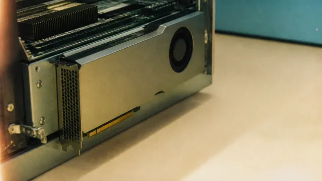
AMD Instinct MI350P: 144GB HBM3E in a PCIe GPU
AMD's Instinct MI350P brings 144GB of HBM3E and 3.6TB/s bandwidth to standard PCIe servers. Here's what it means for the mid-market AI infrastructure gap.

How Optimization Powers Modern AI and Engineering
From training ChatGPT to imaging black holes, optimization is the hidden engine behind modern AI and engineering. Steve Brunton's lecture explains how.